
PHI 700 Scanning Auger Electron Spectrometer
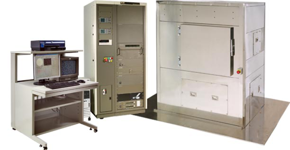
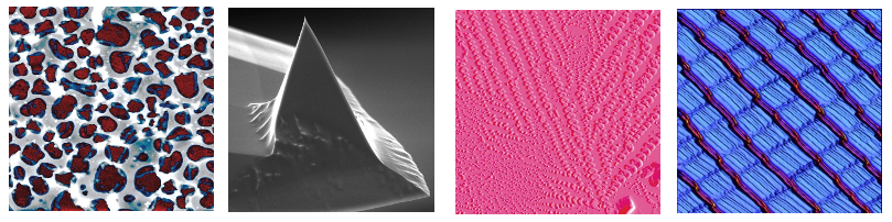
Physical Electronics PHI 700 scanning Auger nanoprobe can be thought of as a scanning electron microscope with a specialized electron energy analyzer for measuring conductive samples with elemental sensitivity 1 to 0.1 atomic percent. The spatial distribution of elements on a surface can be mapped with minimum 20nm lateral resolution and 3nm depth resolution. Changes in elemental composition within the depth of a sample can be documented by recording surface composition while using an ion gun to gradually remove surface layers. The sample is analyzed in an ultra high vacuum chamber.
- Elemental and in some cases chemical analysis
- 20nm minimum lateral resolution
- Elemental sensitivity (1.0 to 0.1 atomic percent)
- 3nm depth resolution
- Conductive samples only; insulators are difficult to analyze
- Argon ion gun for depth profiling and sample neutralization
- Portable transfer vessel to allow samples to be loaded into the instrument without exposure to air
- Nitrogen-coolable impact fracture stage for intergranular fracture surface analysis
Libby Shaw, Research Specialist
Room 13-4137
Email elshaw@mit.edu for training
New PANalytical Empyrean Diffractometer
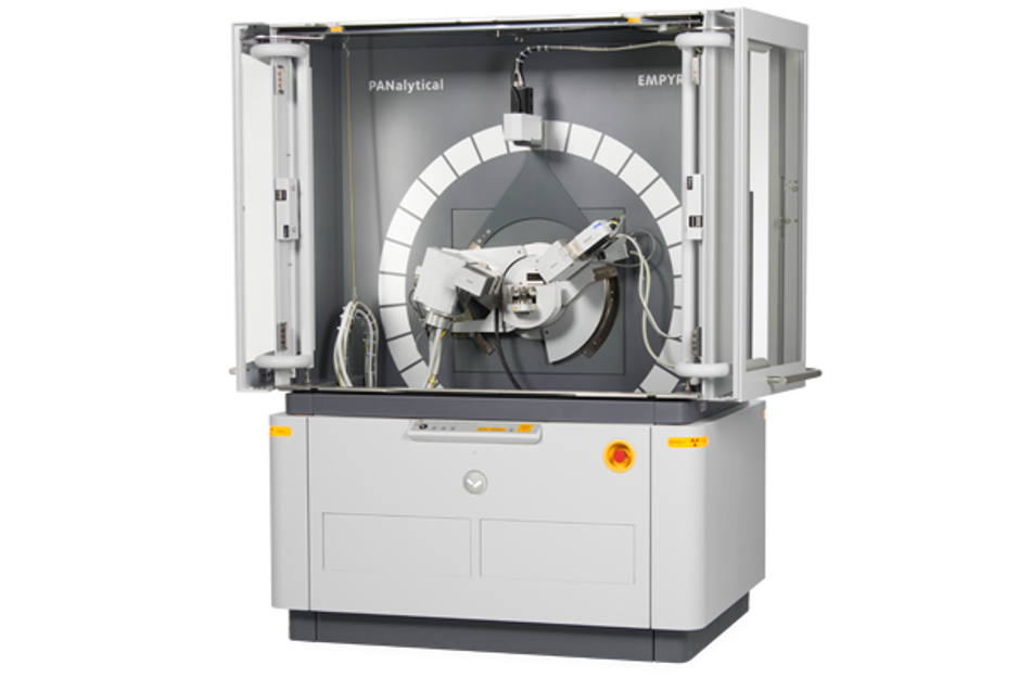
The Panalytical Empyrean diffractometer can be used to quantitatively characterize the phase of solid crystalline materials such as catalysts, corrosion products, metals and alloys, minerals, ceramics, cements, polymers, small organic molecules, and pharmaceuticals.
The current instrument configuration consists of a Cu X-ray source, Bragg- Brentano HD mirror, reflection-transmission spinner stage, 45 position sample changer and a PIXcel 1D solid state detector. There is also an Anton Paar CHC plus+ in-situ heating and relative humidity stage for sample investigations in humid gas, air, inert gas or vacuum. The heating stage can achieve -5 °C to 300 °C in air or inert gas and up to 400 °C in vacuum. Controlled humidity is possible for sample temperatures from 10 °C to 80 °C.
Charles Settens, Research Specialist
Room 13-4027 (X-ray Lab)
Email settens@mit.edu for training
New Bruker Icon Atomic Force Microscope (AFM)
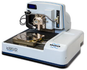
- Magnetic Force Microscopy
- Piezo Force Microscopy
- Conducting atomic force microscopy
PeakForce Tapping mode with ScanAsyst offers extremely low noise imaging of heterogeneous samples
Kelvin Force Probe Microscopy with amplitude or frequency feedback
Electrical characterization from 80 fA to 1 uA with 10 nm spatial resolution
Pixel-by-pixel quantitative force curve characterization to probe material properties
Libby Shaw, Research Specialist
Room 13-4151 (AFM lab)
Email elshaw@mit.edu for training
Modern materials science and engineering requires sophisticated and modern equipment. The Shared Experimental Facilities (SEFs) are designed to address equipment needs too large to be satisfied by individual researchers. The Materials Science and Engineering Center operates four SEFs on the MIT campus for the analysis and processing of materials. These facilities include:
These facilities are available for use by members of the MIT research community and other academic institutions. Use of the facilities is also permitted, consistent with NSF policy (see NSF Important Notice 122*), to qualified research personnel from profit and nonprofit organizations, provided that comparable services are not available on a commercial basis in the private sector.
Our Center is part of the NSF Materials Research Facilities Network.
Read more about our Shared Experimental Facilities in our annual report (PDF).